
Computer Hardware and Architecture - A Bird’s Eye View
In this blog post we take a step lower from our previous blog posts on compilers/virtual machines and operating systems. We will string together how physics and hardware are built and used to execute our abstract thoughts and ideas illustrated in higher level languages.
Post Outline
Introduction
Let’s start with a brief overview of operating systems and compilers before working our way downwards. Here are separate blog posts on the compiler and the operating system that go into more detail.
Operating Systems
At the top is the operating system, which executes user (application developer) programs. The OS is a piece of software built on top of the hardware that abstracts away certain components from the user including process and thread management, the file system, and dealing with memory (instead presenting virtual memory to the user and user processes).
BIOS (Basic Input/Output System) is a set of computer instructions stored in read only memory that performs hardware initialization when the computer is first turned on and sets up the operating system for the user.
Compilers
Next is the compiler, which turns high level source code into low level machine code that an be executed on the hardware. Operating systems are nowadays typically written in mid to high level source code (i.e. C/C++) although the first operating systems were written in machine code. There are some languages like C/C++ that have a compiler that does this translation directly. While this does have certain speed benefits, it is also less portable because a new compiler must be used for each different operating system.
Then there are languages like Java and its famed JVM. Java compilation has two parts: the compilation of the source code into Java bytecode by the compiler and the execution of the bytecode that is interpreted by the JVM. The Java compiler (i.e. the first step) is platform independent and the bytecode of a program can be used on any platform. The JVM is platform dependent since it has to execute for a particular platform. This breaks up the compilation process and allows for more modularity and flexibility.
Assembler
What is an assembler
We get assembly (symbolic) language from the output of the compiler.
Assemblers translate programs written in this symbolic assembly language into binary machine language.
Symbolic assembly language examples include PUSH 0x3 or MOV 0x0 %eax (examples from x86).
For more examples of assembly (specifically x86) and how it is used in when compiling C source code, check out this blog post.
Let’s start by going over what machine code is.
Binary Machine code
Machine code is a series of 1s and 0s that form instructions (and their operands). These instructions make changes to memory using the CPU (i.e. its ALU and the registers). In a 32 bit computer, instructions are 32 bits long. To understand a specific computer’s machine language, we need to know its ISA (instruction set architecture). The ISA is the blueprint of a processor.
There are generally two kinds of ISA’s: RISC (reduced instruction set computer) and CISC (comlex instruction set comptuer). RISC is where less, simpler instructions are used that can execute much faster but at the cost of having to execute more instructions. CISC is when the CPU can execute more complex instructions that take longer than RISC’s simpler instructions.
There are three general categories of commands that an ISA should specify:
- Arithmetic and logic operations (e.g. addition, XOR, etc.)
- Memory access
- Control flow (e.g. looping, finding next instruction, conditionals like if statements)
Let’s take a look at the specific example architecture for the Hack Machine Language introduced in the book The Elements of Computing Systems.
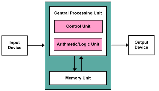
The architecture is a von Neumann architecture, meaning that it has a CPU with a processing (ALU, registers) and control (instruction register, program counter) unit, memory (i.e. RAM), disk storage, and input/output devices (e.g. keyboard, screen).
The architecture has two 16 bit registers (D and A) that can be used by the programmer. D is used to store values (i.e. data register) while A is both a data register and an address register (meaning that the value in register A can be interpreted as an address in memory).
The ISA of the Hack computer architecture has two types of instructions: the A instruction and the C instruction. The A instruction is used to set the A register. Since an instruction is 16 bits on this architecture and the first bit is set to 0 to denote an A instruction, we have 15 remaining bits to represent a value to set the value in the A register to.
The C instruction performs computations, stores the result of those computations somewhere, and decided where to jump next (instruction-wise). The first bit is a 1 to denote that the instruction is a C instruction. Then the remaining bits are divided into the computation, the destination, and the jump. The computation is 7 bits long, the destination is 3 bits long, and the jump is 3 bits long. Each different combination of bits for each of these parts correspond to something different. For example one combination of bits for the computation might indicate that we want to add the values in D and A while another might indicate that we want to AND their values. Then a particular combination of the destination bits might tell us to store the result in the A register, D register, somewhere in memory, or a combination. Then a combination of bits in the JMP mnight tell the CPU to do an unconditional jump to whatever value is stored in the A register. Note that A can be used for deciding wheter to cause a JUMP or as a data memory location for an instruction so well written machine code should make sure that the two are never used in the same program.
How does an assembler turn symbolic assembly into machine code
The assembler is at its core a text processing program that loops through the mnemonic instructions in the assembly and resolves all symbolic referneces to any addresses. A symbol table is typicaly used to store and get addresses corresponding to symbols. The output result is the binary code of the entire program.
CPU
Now that we know what machine code looks like and how we got machine code from the symbolic assembly (which came from the virtual machine of the compiler), how does the machine code actually get run? To answer this question, lets discuss what a CPU has and related components (i.e. memory, I/O devices).
von Neumann Architecture
The von Neumann architecture has the following parts:
- CPU
- processing unit: ALU + Processor Registers
- control unit: instruction register, program counter
- Memory (RAM)
- Mass storage (hard drive)
- input/output devices
The CPU (i.e. the central processing unit) is made up of two parts: the processing unit and the control unit. The processing unit has the ALU (arithmetic logic unit) and multiple processor registers. The control unit has a instruction register (holds current instruction being executed) and a program counter (keeps track of next instruction to execute). The CPU performs “basic arithmetic, logic, controlling, and input/output operations specified by the instructions in the program” (Source). The memory (Random Access Memory) stores the program’s data and instructions. There is also mass storage in the form of hard drives and disks that make up non volatile memory. Then there are input/output devices like the keyboard and the display.
There are two kinds of computers: general purpose (e.g. Windows, Apple) or dedicated computers (e.g. game consoles, factory equipment, phones, digital camera). Both categories have this idea of stored programs in a von Neumann architecture.
Note that modern computers will have a graphics card, which performs graphics computations (such as drawing lines on screen) instead of the CPU. The CPu sends the instructions to the graphics card instead of performing graphics computations itself.
How CPU executes machine code
To execute machine code, CPU’s typically follow the instruction cycle: fetch the next instruction to execute, decode it, and execute it. Depending on the computer architecture, multiple instructions may be completed in a single clock cycle or a single instruction may take multiple clock cycles. Each of these sections are described in more detail below.
Fetch
The fetch cycle fetches the next instruction to execute. This will depend on whether the current instruction said to jump and also the ALU output. The program counter is then set based off of those two factors. The program counter (i.e. instruction address register) is wired to main memory and gets the value (an address) stored at the address represented by the value in the program counter. The value at the address retrieved is the instruction and is loaded into the instruction register.
The next iteration of this cycle will then have the program counter pointing to the next instruction to execute.
Decode
Instruction decoding involves parsing the input instruction (represented in machine code) into the operator and its corresponding operands if any. This is done using the ISA. The control unit (built out of circuits) performs the decoding and determines what instruction will be executed.
Execute
During the execution step in the cycle, different parts of the chip are signaled to execute the instructions. This is done by routing the bits decoded into its separate parts in the decode step to their proper destinations. The CPU already knows what to do for each instruction; it just needs to be told which instruction. The instructions fed in cause certain transistors to open or close which connect the correct circuitry.
Storing Data
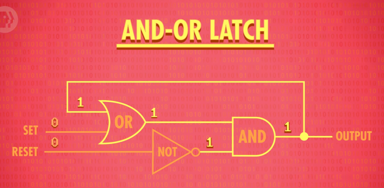
Storing data amounts to storing bits (1s and 0s). We will look at how RAM works (memory that is used when the power is on as opposed to persistant storage such as disk). RAM stands for Random Access Memory. It is called this because memory can be accessed at any address in any order (i.e. randomly). Let’s look at a specific type of RAM: SRAM (static random access memory). SRAM uses latches to store bits. A latch is a circuit that “latches” onto a particular value. Below is an example of an AND OR latch with two inputs: set and reset. Setting set to 1 sets output to 1. Setting reset to 1 resets output to 0. If neither are set then the latch outputs the last output.
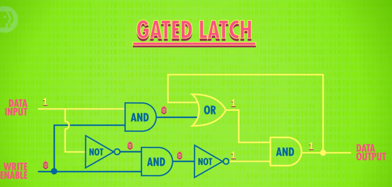
A gated latch adds several gates to the AND OR LATCH that modify the inputs to be data input and write enable. The output of the gated latch is set to the data input only if the write enable wire is set.
These gated latches are put into a matrix so that we can efficiently have lots of memory with minimal wiring required. We can use a multiplexer (gate that combines many inputs into a single output) to get the index for a specific row and column in the matrix.
ALU Computations
The ALU (arithmetic logic unit) is the part of the CPU that performs all the calculations a computer needs to make. It is built with boolean logic gates made out of transistors that are described in the next section.
How does an ALU perform computations
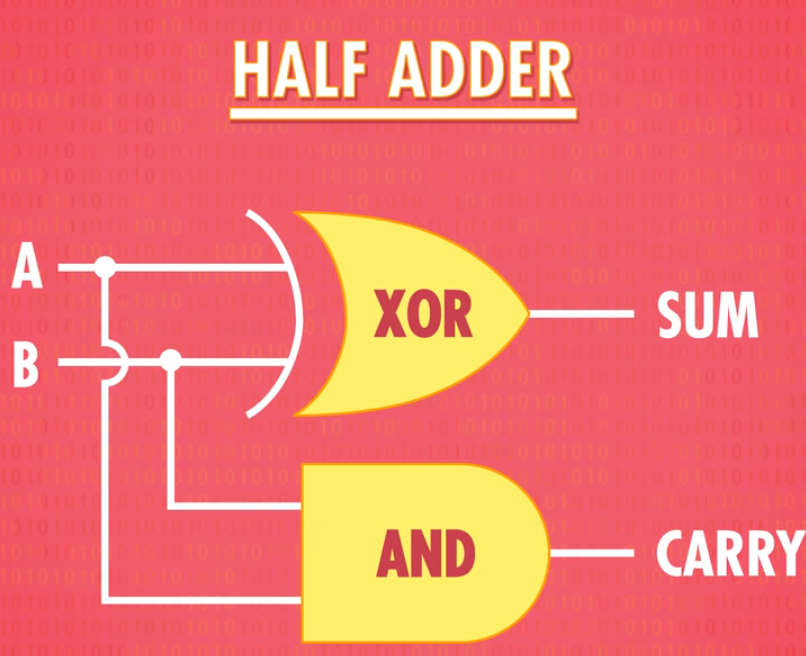
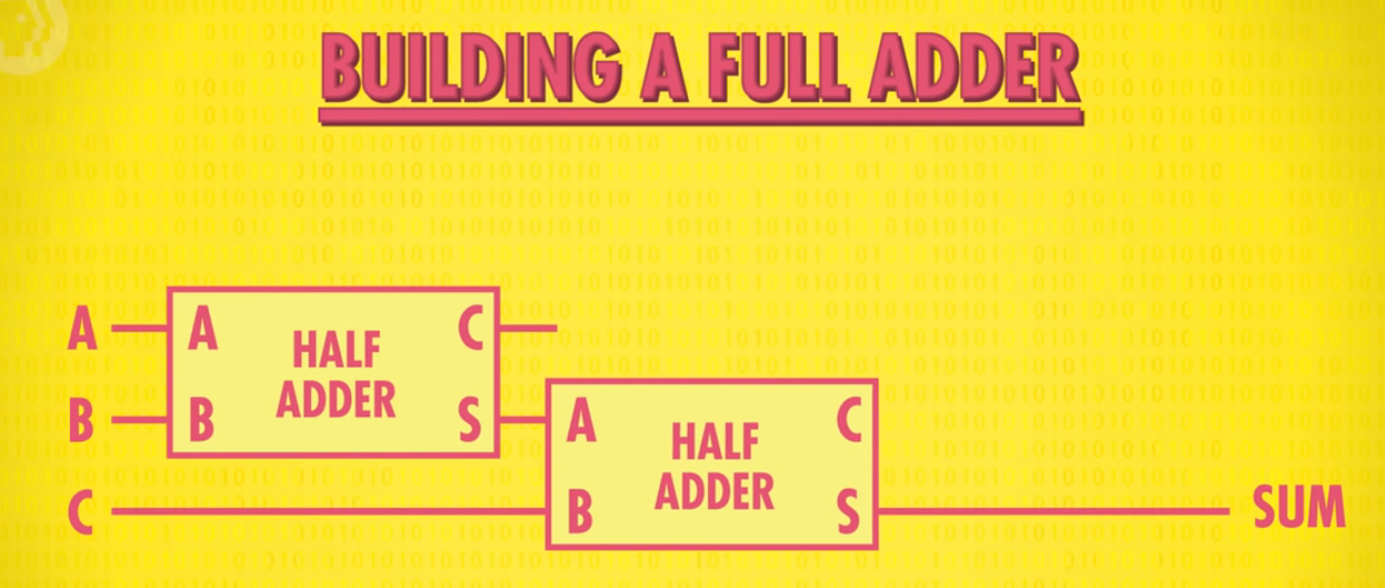
The ALU can perform two types of computations: arithmetic (e.g. addition, subtraction, increment) and logical (e.g. AND, OR, NOT). Let’s take a look at how to add two numbers together. We will be building the addition circuitry out of AND and XOR gates. The first step is a half adder, which essentially adds two single bit numbers together and outputs a single carry bit. The carry bit is set if the inputs are 1 and 1 (resulting in the need to carry).
To build a Full Adder that can add numbers with more bits together, we can combine Half Adders. Full adders take in three single bit inputs and output a carry bit and a sum. Full adders are built using two half adders:
To build a full 8 bit adder, we can combine 1 half adder and 7 full adders like so:
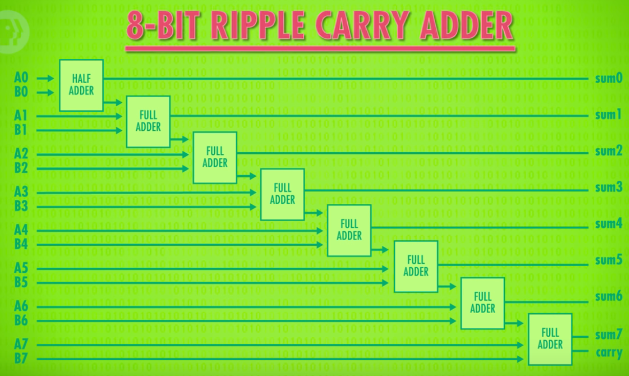
This is called a ripple carry adder. Because it takes time for the carrys to “ripple” across, modern computer use a more complicated carry look ahead adder.
Note that the adder can also be used to perform more complicated operations like multiplication. While computer chips in simpler devices like TV remotes will use the adder for multiplication, laptops and mobile devices will most likely have dedicated chips to performing multiplication (RISC vs CISC).
In addition to arithmetic computations like addition, the ALU can also perform logical computations like AND, OR, NOT, checking if a number is negative, and more. Hence the ALU gets its name of Arithmetic AND Logic Unit.
An 8 bit CPU’s ALU could look like the following:
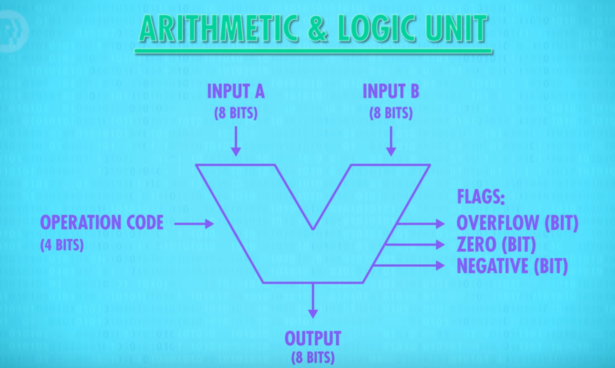
We have two inputs each of 8 bits. There is an operation code that specifies the operation we want to perform. For example 0100 might correspond to the ADD operation. The output is the output of the 8 bit operation (also in 8 bits). There are also flag outputs that may be set depending on the output. For example the zero bit will be set if the output is 0.
Transistors
A transistor is essentially a switch that can be turned on or off with a very weak electrical charge. A transistor has two electrodes and a control wire. If the control wire is turned on, electricity is allowed to flow from one electrode to another.
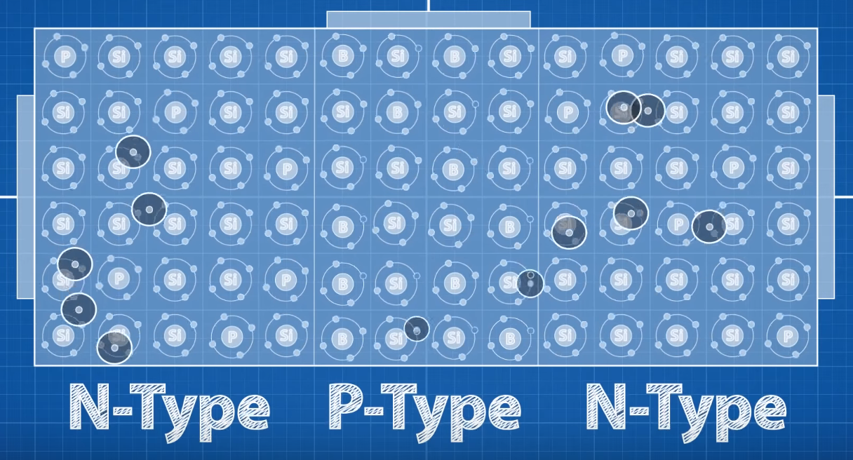
Silicon is used to build these transistors. Silicon is a semi conductor, which means that can partially conduct electricity. A transistor is made out two negatively charged parts separated by a positively charged part. The boundaries between the negatively and positively charged parts prevent the flow of electrons. This is because of the electrons flowing away from the middle positively charged part towards the side and repelling electrons trying to cross. If a positive voltage is applied through the input, it cancels out the electrons repelling the current and allows electrons coming from one end to the other.
Below are some elementary gates from which more complex composite gates can be built out of. Note that gates today are usually designed on hardware simulators using a Hardware Description Language (HDL) like Verilog.
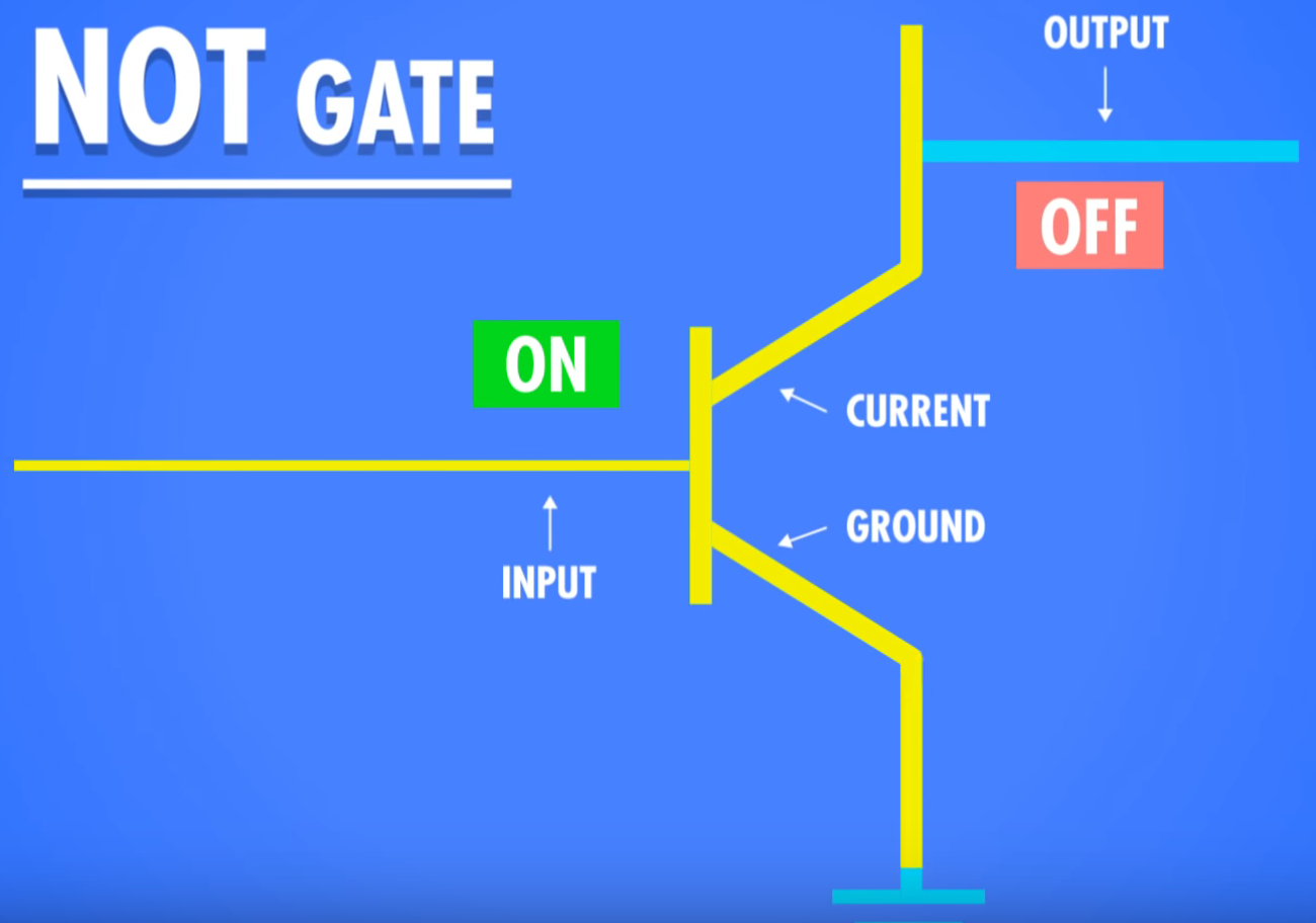
Not Gate
In a not gate, we have an output wire extend from the top input wire. If the input is on, the top current electrode is connected to the ground and the output remains off. If the input is off, the top electrode isn’t connected to the ground so it goes through the output, turning it on.
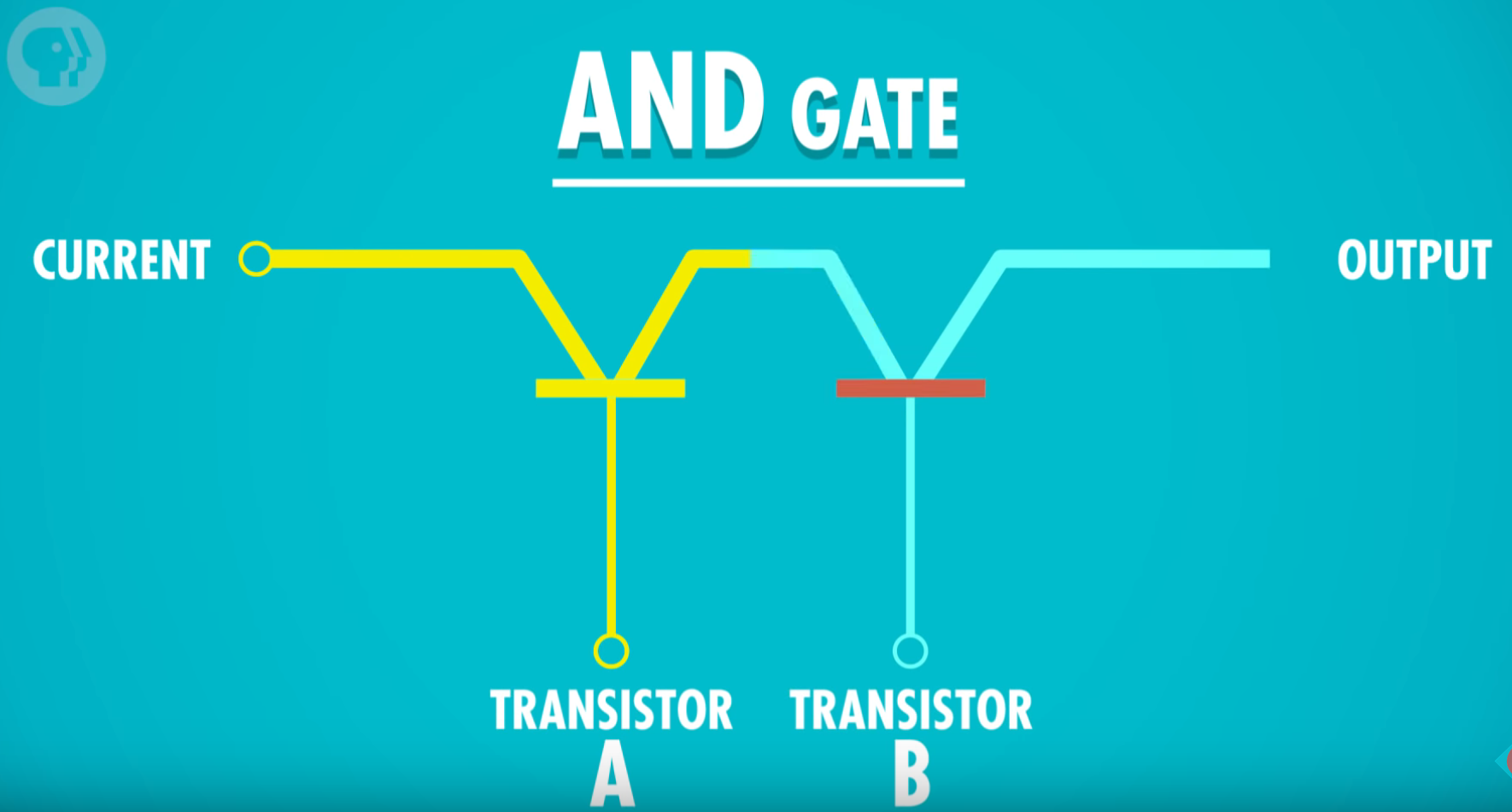
And Gate
To create an AND gate, we can connect two transistors in series as shown below. It can be seen that the inputs for both transistors need to be turned on in order for current to flow to the output wire.
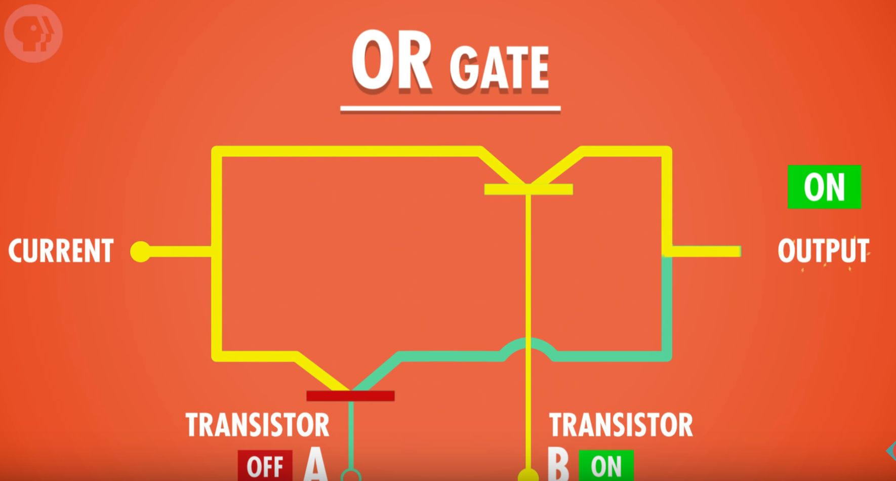
Or Gate
To create an OR gate, we connect two transistors in parallel. From the below diagram, we can see that if either transistor’s input is on, current will flow from the left side to the output wire.
Conclusion
In this post, we began from higher level abstractions (i.e. the operating system and the compiler) and worked our way down through the assembler and the processor architecture all the way to the physical level (i.e. transistors).